Validation Gets Tested At 1kW

Key Takeaways:
- 1kW is not a single validation condition. Workload, location, temperature, and time all change the stress being applied to chips.
- Test hardware can become part of the reliability problem when contacts, sockets, load boards, and thermal-control systems change under sustained high current.
- Coverage has to extend beyond fault detection and include thermal, workload, timing, and field data to understand whether a device is actually reliable.
On a spec sheet, 1kW of maximum power looks like a single operating condition. In practice, two workloads can hold an AI accelerator at the same power level while driving different compute blocks, memory interfaces, and power-delivery paths. Power moves even when the number doesn’t, and heat moves with it.
That makes validation more than reproducing the rated power. The device is only one part of the physical system that carries and removes that power.
“At these kilowatt-class power levels, we’re essentially validating not only the device itself, but the entire package, the cooling, the test ecosystem itself,” said Christopher Rand, principal technical engineer at Nordson Test & Inspection. “The tools that we’re using in that ecosystem are very much part of the system that we’ve got to qualify and validate.”
Validation has always depended on coverage. Engineers build test patterns to expose faults, exercise a range of operating conditions, and push a device toward its limits. But at sustained loads approaching 1kW, a passing electrical result no longer guarantees the device was tested in the state it will actually run in.
“This is a new trend in AI,” said Brent Bullock, test technology director at Advantest. “We normally look at fault coverage, but now we have to start thinking about correlating fault coverage with thermal coverage. We can’t just look at fault coverage alone. We have to look at fault coverage and thermal coverage collectively.”
That widens the job considerably. A test can exercise the right logic without applying heat in the same places as real workloads, or keep it there long enough for the resulting electrical and thermal behavior to develop.
The problem starts in the transient analysis before silicon ever reaches the tester. Engineers have to model how the accelerator will behave as workloads change over time, not just at a fixed current and temperature. Different parts of the device become active at different moments, and a workload that passes in one combination can expose a different margin in another.
“For transition, it’s all about coverage,” said Lang Lin, principal product manager at Synopsys. “For some particular load you fail, for some other load maybe you still pass, but the chip actually is in a very bad situation. Reliability-wise, it will tend to fail later.”
That is what makes 1kW more interesting than the number itself. A short test may prove that the device can operate safely under a condition. It doesn’t prove the test exercised the right combination of workload, location, temperature, voltage, and time that eventually sets the reliability limit. The useful question is no longer just what happens at a specified operating point, but what happens along the way.
What counts as coverage now?
One obvious approach for validating a high-power accelerator would be to push everything as hard as possible and watch what happens. But “everything on” is not necessarily what the device will experience in service, and some test methodologies have spent years moving in the opposite direction.
Scan is a good example. Power-aware scan has become increasingly important because excessive simultaneous switching can create conditions that don’t represent functional operation. That makes scan well suited to finding structural faults, but less useful when the goal is to reproduce a particular high-power thermal condition. Mission-mode and built-in self-test can get closer to how the device will actually operate, but they still have to reproduce a workload that creates the conditions engineers need to validate.
A workload can look representative in aggregate and still stress the device in the wrong places. Worst-case power is useful for bounding a design, but a single package-level number says little about where hot spots will concentrate. Large guard bands can compensate for some of that uncertainty, but on an AI accelerator that margin often comes at the expense of performance.
“The engineer has to stop assuming that worst-case power at this temperature is the criterion to safely sign off on a chip,” Lin said. “They need to know where the 1,000 watts are distributed on their die, because the total number doesn’t mean anything.”
That pushes validation beyond aggregate limits and toward what is happening locally under a real workload. A surface temperature may look acceptable while a much smaller region is running hot enough to affect timing or long-term reliability.
“Today, a spreadsheet is not enough,” Lin said. “You’re going to use your real design, run the workload, give the stimulus, and measure temperature everywhere. You have to have data to back up your system design quality.”
Time runs at different speeds
How long a device has to remain at high power depends on what engineers are trying to expose. Some problems develop almost immediately, while others appear only after the test interface itself has had time to heat and change. At package test, where the assembled device can draw substantially more power than an individual chiplet at wafer sort, the first problem may arrive very quickly.
“A chip can go into thermal runaway within a few hundred microseconds,” said Bullock. “You have to be able to react very quickly. We can watch the voltage drop across the contact, and if the current starts running away, which is indicative of thermal runaway, then we can shut things down. You want to be able to stop it before it does too much damage.”
Catching that excursion requires fast detection, but surviving the first few hundred microseconds doesn’t mean the electrical path will remain stable. Sustained current begins heating the contacts carrying it, raising their resistance and gradually changing the conditions under which the device is being tested.
“When current is applied for a long duration, seconds, it causes the pin temperature to increase, which also increases the contact resistance, thus limiting the contact’s current-carrying capacity,” said Glenn Cunningham, director of test and characterization at Modus Test. “This also happens when current is applied briefly in shorter durations — milliseconds — albeit not as quickly.”
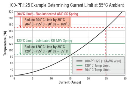
Fig. 1: Higher ambient temperature reduces the thermal margin available to a test contact, lowering the current it can carry before reaching its specified temperature limit. Source: Modus Test
A contact can therefore look healthy at the beginning of a test and fail only when it is asked to carry realistic current.
“As long as the pin is in contact with the PCB and the DUT, it may pass initial continuity, opens/shorts test, depending on the limits set in the test program,” Cunningham said. “However, when the current is applied, it may fail.”
Beyond that, validation runs into a practical limit. Some reliability effects develop over repeated workloads or much longer periods than production test can reproduce. Accelerated qualification can compress part of that history, but manufacturers still have to balance how long they exercise a device against how quickly it has to move into production.
So how long can an OSAT realistically exercise a kilowatt-class device? “Not long enough,” said Brad Booth, CEO of NLM Photonics. “OSATs do their basic test, do a burn-in and say, ‘Okay, yeah, we think the structure of this should be fine,’ but speed of delivery is critical. No one is going to run these systems ad infinitum to make sure that they live forever.”
That means validation must cover an enormous span of time. One problem can become dangerous in a few hundred microseconds. Another may need seconds of sustained current before a contact has heated enough to change resistance. Others might emerge through repeated workloads, accumulated thermal cycles, or during operation, long after qualification is complete.
No single dwell time can cover all of that. The job is to know which clock matters for the mechanism being tested, what evidence appears on that clock, and whether the test still means the same thing after the rest of the hardware has had time to respond.
But that leads to another problem. At these power levels, the accelerator is not the only thing being stressed. The load board, contacts, thermal-control hardware, and ATE all have their own limits and their own time-dependent behaviors. Before engineers can trust a failure, they increasingly need to know which part of the stack caused it.
The full stack gets a vote
At some point, a kilowatt stops being only the DUT’s problem. Power has to travel through the test path before it reaches the device, and that path is not electrically or thermally neutral. Changes anywhere along it can alter the condition the DUT actually sees.
“Historically, we could separate the load board and the tester and the prober or the handler and kind of treat everything separately,” said Advantest’s Bullock. “But we’re to the point now with the wattages that we’re dealing with that we really need to look at the full stack.”
At these power levels, the test hardware becomes part of the experiment. Its own electrical and thermal behavior can shift the condition at the DUT, so engineers need enough visibility to know whether an apparent anomaly began in the silicon or somewhere along the delivery path. That puts more emphasis on characterizing the test system under load and verifying what actually reaches the device.
“It’s kind of like a three-way dance right now,” said Damian Megna, product manager for power and thermal instrument solutions at Teradyne. “The end customers are looking to us for solutions, but we have to work with handler and prober companies that have access to the cooling technology that touches the package. We have to work together to provide a total solution. It’s just not progressing fast enough to keep up with how fast advanced packaging is evolving in terms of thermal requirements.”
The device-under-test and test interface can also begin affecting each other under load. Current doesn’t always divide evenly among identical power contacts. Small differences in resistance can direct more current through one path, heating it further and changing the distribution again.
“Current is spread across all contacts, but not equally, as each contact has its own resistance,” said Modus Test’s Cunningham. If several contacts develop higher resistance while one remains much lower, most of the current can concentrate through that lower-resistance path. “This will create what is referred to as EOS (electrical overstress) and is catastrophic to the contact, socket, and device under test.”
What the package remembers
The package adds another layer to the problem. High current creates local heating, and that heat can change both electrical behavior and the physical structure around the device. Effects that are convenient to analyze separately can begin feeding back into one another under sustained load.
“Regardless of workload dependency, the physics still couples with each other,” said Synopsys’ Lin. “A stress change could change the mobility of the transistor, and change the performance as well. So it’s a big loop — power, thermal, timing, and stress.”
The practical question is when those transient changes stop being merely transient. A hot spot that comes and goes may leave no lasting damage. Repeated heating becomes more consequential if it begins changing an interface or interconnect in a way that persists after the workload moves elsewhere.
“The most concerning defects — the ones that will give you an operational problem down the line, particularly after a lot of thermal load and cycles — tend to be smaller defects,” said Nordson’s Rand. “These are not the big gross defects that would make a device fail outright at the beginning.”
Those early signatures can include voiding, early delamination, and interfacial cracking. A void reduces the available path for heat conduction, which can create a localized hot spot and compound the thermal problem. Some of those weaknesses may not be visible in initial electrical test.
Mechanical behavior creates another complication. A large package can warp under thermal load and then relax as it cools, even though the stress has already changed an interface somewhere inside it.
“As soon as you remove that device from that situation, you take the heat away, you might lose that warpage,” Rand said. “You might not be able to see that, but the remains of the damage it caused will definitely be there.”
That makes the baseline important. Non-destructive inspection before stressing the package establishes what was already present, followed by inspection after sustained or cyclic loading to determine whether those defects propagated. Acoustic and X-ray inspection provide different views of that process, while destructive analysis can go further when engineers already know what to look for.
Correlation becomes the problem
Better visibility doesn’t automatically make validation easier. Modern accelerators generate enormous amounts of data, often on different time scales. The harder problem is connecting those measurements to the actual workload and operating condition that produced them.
“The timing margin is impacted by many things in a system,” said Alex Burlak, executive vice president of engineering and customer success at proteanTecs. “It’s impacted by IR drop. It’s impacted by temperature. It’s impacted by process. It’s impacted by degradation.”
That makes timing margin useful as a window into the device rather than as an isolated measurement. Engineers can compare where it changes with what the logic was doing at the time to begin separating a real weakness from normal variation.
But individual measurements may not carry enough meaning on their own. A small thermal excursion, marginal void, timing shift, or resistance change may be benign in isolation but more revealing when several parameters begin moving together.
“It’s not quite as straightforward as, ‘If I see this, then I know this is going to happen,’” Rand said. “It can be a combination of things that, statistically speaking, will point toward something that is going to happen later on. It’s finding those trends.”
Those relationships also give engineers something more useful to model. An unexpected result becomes more than an outlier if it exposes a condition or interaction the simulation did not predict.
“We’re putting more emphasis on simulation and modeling now so that we discover these issues and pay more attention to them early in the cycle before the hardware is designed,” Bullock said.
The closer those models can get to the conditions that actually produce failures, the more useful each generation of validation becomes in shaping the next.
Validation follows the device
There is still a point where the accelerator has to leave the lab. No amount of qualification can reproduce years of operation under every workload and system condition it will encounter. Development cycles are moving too quickly for that. Some of the information engineers would like to have before release is still being gathered while the next design is already underway.
“It’s very hard then to spend money on the research side to actually start pushing some of the technology and start finding the corner cases early, which is critical, especially when we look at building some of these GPU, CPU kilowatt-type devices,” said NLM Photonics’ Booth.
Some of those corner cases will appear only in the field, where the accelerator is operating as part of a much larger system. A failure that looks like a chip problem may originate somewhere outside the device or only after interactions that qualification couldn’t reproduce.
“There is always something that can happen in the field, whether it’s defects that weren’t identified or some systematic issues that take more time to manifest,” said proteanTecs’ Burlak. “There are also interactions between the chip and the system, and the system and the data center, that are very hard to mimic in the validation phase.”
That puts a limit on what engineers can learn from a finite test window. Some of the visibility used during validation therefore has to follow the device into operation.
“You first need to know what’s happening inside the chip on a large scale, and monitor that,” Burlak said. “It’s not enough to collect voltage and temperature from the chip or from the system. You need to collect timing margin information, IR drop, voltage droop information, and cycle-to-cycle jitter.”
Conclusion
It’s tempting to look at a 1kW accelerator and conclude that validation simply needs more of everything — more current, more cooling, higher stress, longer dwell times, and more test. Some of that will certainly be required, but it misses the harder part of the problem.
A kilowatt power ceiling is not one condition, and no single test is long enough, hot enough, or aggressive enough to represent everything that can happen at that level. One failure precursor can appear within hundreds of microseconds while another develops as contacts and boards warm over time. Workload can move a hot spot before the rest of the package reaches equilibrium. The test hardware can change underneath the measurement. Other effects may not become obvious until thousands of deployed devices have accumulated histories no laboratory could afford to reproduce.
The real change is in what engineers mean by coverage. Electrical fault coverage still matters, but it increasingly has to line up with thermal coverage, workload coverage, spatial coverage, and enough time-domain information to know which failure mechanism is actually being exercised.
Related Articles
When The Test Cell Lies
As margins shrink and dies move into expensive packages, separating device failures from test-cell artifacts has become a first-order economic problem.
AI Accelerator Testing Depends On DFT Innovations
Multi-die assemblies greatly increase the number of things that can go wrong, and the difficulty of finding them.
How Long Does A Measurement Remain Valid?
Measurements can be misleading after the chip, the test path, or the assumptions behind the result change.
The post Validation Gets Tested At 1kW appeared first on Semiconductor Engineering.