Streaming Scan Network Test Over PCIe

Every generation of AI and data center silicon brings more logic, more cores, and more scan content that has to reach the device for test. Chiplet-based packages compound it, because each die arrives with its own test requirements and its own patterns. DFT and test engineering teams need better solutions to get content to the device fast enough to keep test time and test cost in line.
One such solution is Siemens’ Tessent Streaming Scan Network, which packetizes scan data so it can be delivered efficiently and shared across cores. Tessent In-System Test builds on this by adding an on-chip controller that accepts deterministic patterns over a standard AXI bus, meaning test content can arrive through a functional interface the device already carries, such as PCIe or USB, rather than through a dedicated test port.

Fig. 1: In-System Test Controller (ISTC). Source: Teradyne
Utilizing this approach with Teradyne UltraFLEXplus results in a combined solution leveraging a programming model test engineers already use. Teradyne has integrated Siemens Tessent Silicon Executable into the UltraPort server and the IG-XL software on UltraFLEXplus. Content generated in the Tessent shell flow is delivered to the device over the device’s own PCIe interface through UltraPort, and the test is set up, executed, and debugged inside the standard IG-XL programming model. Failure data returns in the formats the Tessent diagnosis ecosystem already consumes, so established yield and failure analysis flows carry straight over.
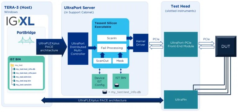
Fig. 2: Tessent Silicon Executable running on the UltraPort Server. Source: Teradyne
Teradyne and Siemens EDA have been building joint solutions since 2000, when built-in self-test first met automatic test equipment. In 2019, the two companies simplified silicon bring-up and debug on ATE through Tessent ATE-Connect and Teradyne’s PortBridge. More recently the work has centered on running Streaming Scan Network content on UltraFLEXplus. Each step has followed the same principle: design-for-test decisions and test execution should not be two separate conversations held by two separate teams many months apart.
For a team adopting SSN over a high-speed interface, the practical gains are continuity and support. One programming model carries from engineering bring-up through production. Patterns and diagnosis flows established during design stay usable at the tester. And when something needs attention, the hardware, the embedded software, and the integration between them are supported as one robust solution.
With this solution:
- Scan content moves over a high-bandwidth interface the device already carries, which keeps test time in line as pattern volume climbs.
- Bring-up and debug move faster, because patterns can be patched and re-run inside the same flow that generated them, and failure data comes back in the formats the diagnosis tools have already read.
- Deterministic EDT patterns can be applied at ATE, SLT and in-system, so pattern content can be updated as new fault models emerge.
- The DFT work a design team has already done in Tessent carries forward to the tester, to the bench, and into the system, with one place to go when something needs support.
The AI buildout has changed what a test strategy has to account for. Devices are larger, draw more power, and are increasingly assembled from chiplets, where a single weak die can compromise a package worth many times its own value. Decisions that set test cost are being made earlier, inside the design flow, by teams choosing DFT architecture long before a device reaches a tester. That shift left puts a premium on how closely the design ecosystem and the test ecosystem line up. When the DFT tool and the test platform are engineered to the same interfaces, the work a team does on the design side converts directly into production capability, and the path from architecture decision to tested silicon stays short.
The post Streaming Scan Network Test Over PCIe appeared first on Semiconductor Engineering.